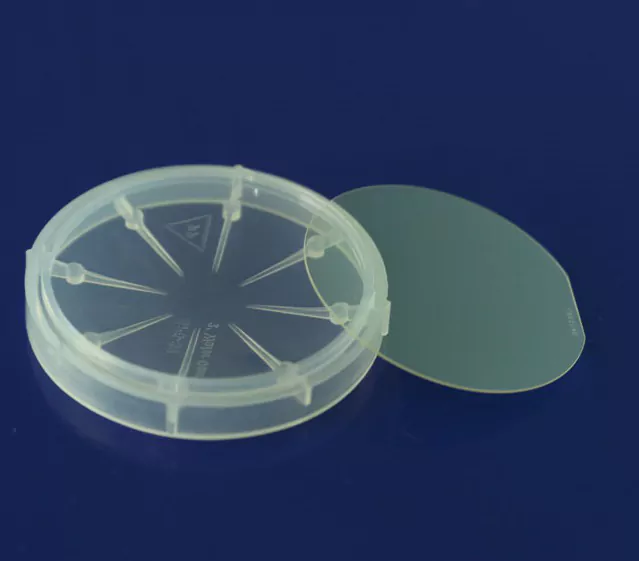
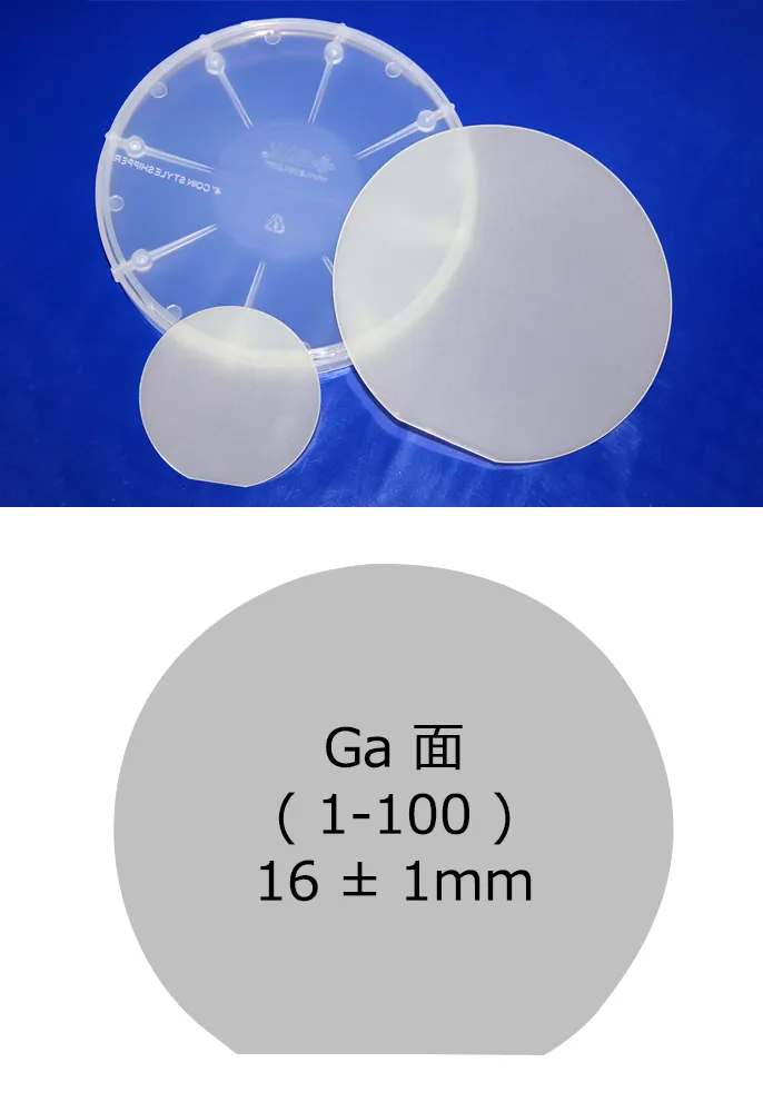
GaN基板
| 項目 | 仕様 | ||
|---|---|---|---|
| 直径 | 51.0 mm ± 0.3 mm | 100.2 mm ± 0.3 mm | |
| 厚さ | 490 µm ± 30 µm | 540 µm ± 30 µm | |
| 面方位 | (0001) Ga-Face c-plane | ||
| TTV (5 mm edge exclusion) | ≤15 µm | ≤30 µm | |
| Warp (5 mm edge exclusion) | ≤20 µm | ≤80 µm | |
| Bow (5 mm edge exclusion) | -10 µm to +5 µm | -40 µm to +20 µm | |
| 電気特性 | タイプ | 抵抗率 | |
| N-type (Si) | ≤0.02 Ω·cm | ||
| UID | ≤0.2 Ω·cm | ||
| Semi-Insulating (Carbon) | >1E8 Ω·cm | ||
| グレード | Density (pits/cm2) | 2" (pits) | 4" (pits) |
| Production | ≤0.5 | ≤10 | ≤40 |
| Research | ≤1.5 | ≤30 | ≤120 |
| Dummy | ≤2.5 | ≤50 | ≤200 |
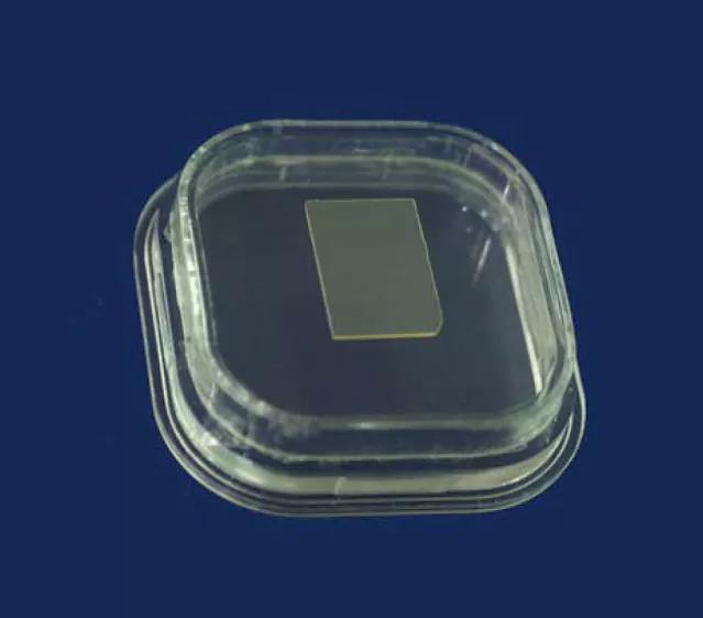
GaN基板(正方形)
| 項目 | 仕様 | ||
|---|---|---|---|
| サイズ | (10 ± 0.5) × (15 ± 0.5) mm2 Customized Size |
||
| 厚さ | 400 ± 25 µm | ||
| 面方位 | C-plane (0001) off-angle toward M-axis 0.35 ± 0.15° or 0.55 ± 0.15° |
||
| TTV | ≤10 µm | ||
| BOW | ≤10 μm | ||
| タイプ | UID | N-type (Si) | Semi-Insulating (Carbon) |
| Ga face surface roughness | <0.3 nm (10 × 10 μm) | ||
| N face surface roughness | Etched (0.5–1.5 µm); Polished (<0.3 nm) | ||
| 転位密度 | <1 × 106 cm2 | ||
| (002) FWHM | ≤70 arcsec | ||
| (102) FWHM | ≤70 arcsec | ||
| Macro defect density(hole) | <0.3 cm-2 | ||
| 有効面積 | >90% | ||
GaNテンプレート(φ2インチ)
| 項目 | 仕様 | |
|---|---|---|
| 直径 | φ50.8 mm ± 0.1 mm | |
| GaN膜厚 | 4 µm、10~25 µm | |
| 方位面 | C面(0001)面 ± 0.5° | |
| タイプ | UID | N-type (Si) |
| オリフラ方位。長さ | オリフラ方位(1~100)。オリフラ長さ 30 mm ± 1 mm | |
| 電気抵抗率(300 K) | <0.5 Ω·cm | <0.05 Ω·cm |
| 転位密度 | 5 × 108 cm2 | |
| 基板構造 | GaN/サファイアウェーハ(0001)面 | |
| 有効面積 | 90%以上 | |
| 表面仕上げ | Ga面:CMP仕上げ。N面:ファイングランディング(オプション:光学鏡面仕上げ) | |
GaNテンプレート(φ4インチ)

| 項目 | 仕様 |
|---|---|
| 直径 | φ100 mm ± 0.1 mm |
| GaN膜厚 | 4 µm、10~25 µm |
| 方位面 | C面(0001)面 ± 0.5° |
| 導電タイプ | N型(Undoped) |
| オリフラ方位。長さ | オリフラ方位(1~100)。オリフラ長さ 30 mm ± 1 mm |
| 電気抵抗率(300 K) | <0.5 Ω·cm |
| 転移欠陥密度 | 5 × 10⁸ 個/cm2以下 |
| 基板構造 | GaN/サファイアウェーハ(0001)面 |
| 有効面積 | 90%以上 |
| 表面仕上げ | Ga面:CMP仕上げ。N面:ファイングランディング(オプション:光学鏡面仕上げ) |
2-inch GaN-on-Sapphire Blue/Green LED Wafer

| Substrate | Type | Flat Sapphire | |
|---|---|---|---|
| Polish | Single Side Polished (SSP)/Double Side Polished (DSP) | ||
| Dimension | 50.8 ± 0.2 mm | ||
| Orientation | C-plane (0001) off angle toward M-axis 0.2 ± 0.1° | ||
| Thickness | 430 ± 25 mm | ||
| Epilayer | Structure | 0.2 μm pGaN / 0.5 μm MQWs / 2.5 μm nGaN / 2.0 μm uGaN | |
| Thickness | 5.5 ± 0.5 μm | ||
| Roughness(Ra) | <0.5 nm | ||
| Dislocation density | <5 × 108 cm2 | ||
| Wavelength | Blue LED | Green LED | |
| 465 ± 10 nm | 465 ± 10 nm | ||
| Wavelength FWHMs | <25 nm | <40 nm | |
| Chip Performance | Cut-in Voltage @ 1μA | 2.3~2.5 V | 2.2~2.4 V |
| Useable Area | >90% (Excluding edge and macro defects) | ||
| Package | Packaged in a cleanroom in a single wafer container | ||
4-inch GaN-on-Sapphire Blue/Green/Red LED Wafer

| Substrate | Type | Flat Sapphire | ||
|---|---|---|---|---|
| Polish | Single Side Polished (SSP)/Double Side Polished (DSP) | |||
| Dimension | 100 ± 0.2 mm | |||
| Orientation | C-plane (0001) off angle toward M-axis 0.2 ± 0.1° | |||
| Thickness | 650 ± 25 μm | |||
| Epilayer | Structure | 0.2 μm pGaN / 0.5 μm MQWs / 2.5 μm nGaN / 2.0 μm uGaN | ||
| Thickness | 5.5 ± 0.5 μm | |||
| Roughness(Ra) | <0.5 nm | |||
| Dislocation density | <5 × 108 cm2 | |||
| Wavelength | Blue LED | Green LED | Red LED | |
| 465 ± 10 nm | 525 ± 10 nm | 630 ± 10 nm | ||
| Wavelength FWHMs | <25 nm | <40 nm | ||
| Chip Performance | Cut-in voltage@1μA | 2.3~2.5 V | 2.2~2.4 V | |
| Useable Area | >90% (edge and macro defects exclusion) | |||
| Package | Packaged in a cleanroom in a single wafer container | |||
6-inch GaN-on-Sapphire Blue/Green/Red LED Wafer

| Substrate | Type | Flat Sapphire | ||
|---|---|---|---|---|
| Polish | Single Side Polished (SSP)/Double Side Polished (DSP) | |||
| Dimension | 150 ± 0.2 mm | |||
| Orientation | C-plane (0001) off angle toward M-axis 0.2 ± 0.1° | |||
| Thickness | 1300 ± 25 μm | |||
| Epilayer | Structure | 0.2 μm pGaN / 0.5 μm MQWs / 2.5 μm nGaN / 2.0 μm uGaN | ||
| Thickness | 6.9 ± 0.5 μm | |||
| Roughness (Ra) | <0.5 nm | |||
| Dislocation density | <5 × 108 cm2 | |||
| Wavelength | Blue LED | Green LED | Red LED | |
| 475 ± 3 nm | 521 ± 5 nm | 630 ± 8 nm | ||
| Wavelength FWHMs | <25 nm | <40 nm | ||
| Chip Performance | Cut-in voltage @ 1 μA | 2.3~2.5 V | 2.2~2.4 V | |
| Useable Area | >90% (edge and macro defects exclusion) | |||
| Package | Packaged in a cleanroom in a single wafer container | |||